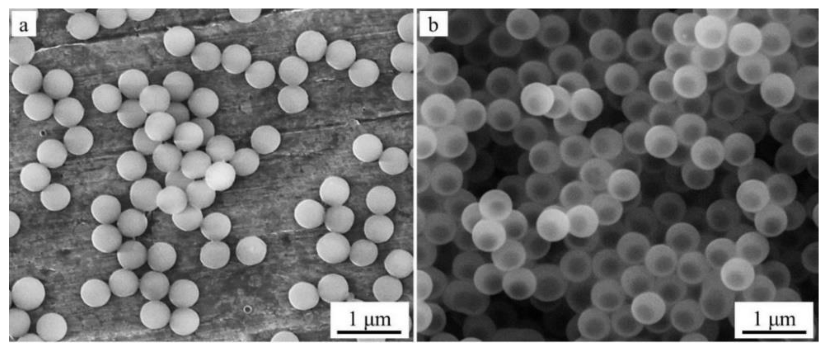
a) SEM image of crystallized silica spheres on a plain Si substrate.

Download scientific diagram | (a) SEM image of crystallized silica spheres on a plain Si substrate. The small black and large white squares represent the areas used for the calculation of the Fourier transforms in Figure 3c and d. (b) Optical micrograph of the etched substrate after the crystallization of silica opals (about 1 mm × 0.7 mm). The high-lying parts of the wafer are uncovered (blank silicon ) white); the low-lying etched pattern is completely filled (dark). (c, d) Representative SEM images showing the same selectivity. Notice the difference between isolated trenches and trenches of the same size, which are connected to a continuous trench in part d. from publication: Integration of Self-Assembled Three-Dimensional Photonic Crystals onto Structured Silicon Wafers | We report on the fabrication of high-quality opaline photonic crystals from large silica spheres (diameter of 890 nm), self-assembled in hydrophilic trenches of silicon wafers by using a novel technique coined a combination of "lifting and stirring". The achievements reported | Silicon Wafer, Photonic Crystals and Self-Assembly | ResearchGate, the professional network for scientists.
Crystals, Free Full-Text

Hollow carbon nanospheres/silicon/alumina core-shell film as an anode for lithium-ion batteries

Porosity and nanostructure of silicon oxycarbide derived carbon - ScienceDirect

Synthesis of Highly Nanoporous β-Silicon Carbide from Corn Stover and Sandstone

Scanning electron micrographs of one monolayer of silica spheres.

Less strained and more efficient GaN light-emitting diodes with embedded silica hollow nanospheres

SEM images of pristine monodisperse spherical silica particles (left)
Frontiers Depletion attraction in colloidal and bacterial systems

SEM Images of silica

Crystals, Free Full-Text
Polymers, Free Full-Text