a) Left: representative SEM image of silica opal on a patterned Si

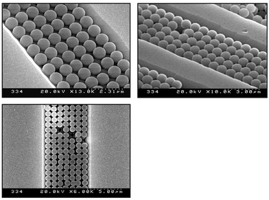
Download scientific diagram | (a) Left: representative SEM image of silica opal on a patterned Si substrate with complex geometry. Right: Fourier transform of a marked region (about 17 spheres × 17 spheres) in an SEM image. (b) Left: SEM image of the same silica opal on another area of the patterned Si substrate. Right: Fourier transform of a marked region (about 38 × 10 spheres) in an SEM image. (c, d) Fourier transform of Figure 1a. (c) Large marked region (about 70 μ m × 50 μ m). (d) Small marked region (about 10 spheres × 10 spheres). from publication: Integration of Self-Assembled Three-Dimensional Photonic Crystals onto Structured Silicon Wafers | We report on the fabrication of high-quality opaline photonic crystals from large silica spheres (diameter of 890 nm), self-assembled in hydrophilic trenches of silicon wafers by using a novel technique coined a combination of "lifting and stirring". The achievements reported | Silicon Wafer, Photonic Crystals and Self-Assembly | ResearchGate, the professional network for scientists.

Nanomaterials, Free Full-Text
Opal chips: vectorial growth of colloidal crystal patterns inside silicon wafersElectronic supplementary information (ESI) available: pictorial repres - Chemical Communications (RSC Publishing) DOI:10.1039/B008534K

Many Facets of Photonic Crystals: From Optics and Sensors to Energy Storage and Photocatalysis - Lonergan - 2023 - Advanced Materials Technologies - Wiley Online Library
Minerals, Free Full-Text

From left to right, scanning electron microscopy (SEM) images of

Influence of pores arrangement on stability of photonic structures during sintering - ScienceDirect

Preparation of Monodisperse Silica Nanoparticles via Controlling the Interphase of Two-Phase Synthesis for Optical Anticounterfeiting Materials

Inkjet Printing Based Mono-layered Photonic Crystal Patterning for Anti-counterfeiting Structural Colors

Colloidal Self-Assembly of Highly-Ordered Silica Inverse Opals for Deep Ultraviolet Diffraction

Colloidal Crystal Films: Advances in Universality and Perfection

SEM images of a cross section (a) of the opal-silica layer-opal

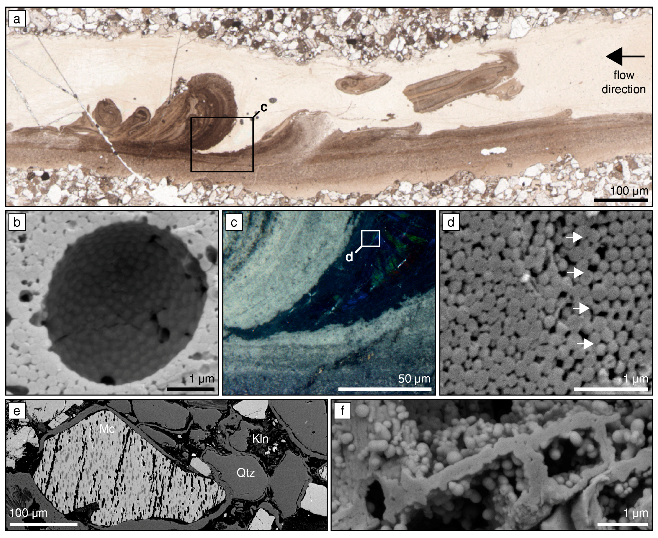
Characteristics and evolution of the Etili silica sinter epithermal deposits, Çanakkale – Turkey: Relation to alkali chloride vs acid-sulfate fluids - ScienceDirect

Left: SEM images of the internal (110) face of silicon in fi ltrated

SEM images of (a) an opal sample consisting of 290 nm diameter silica