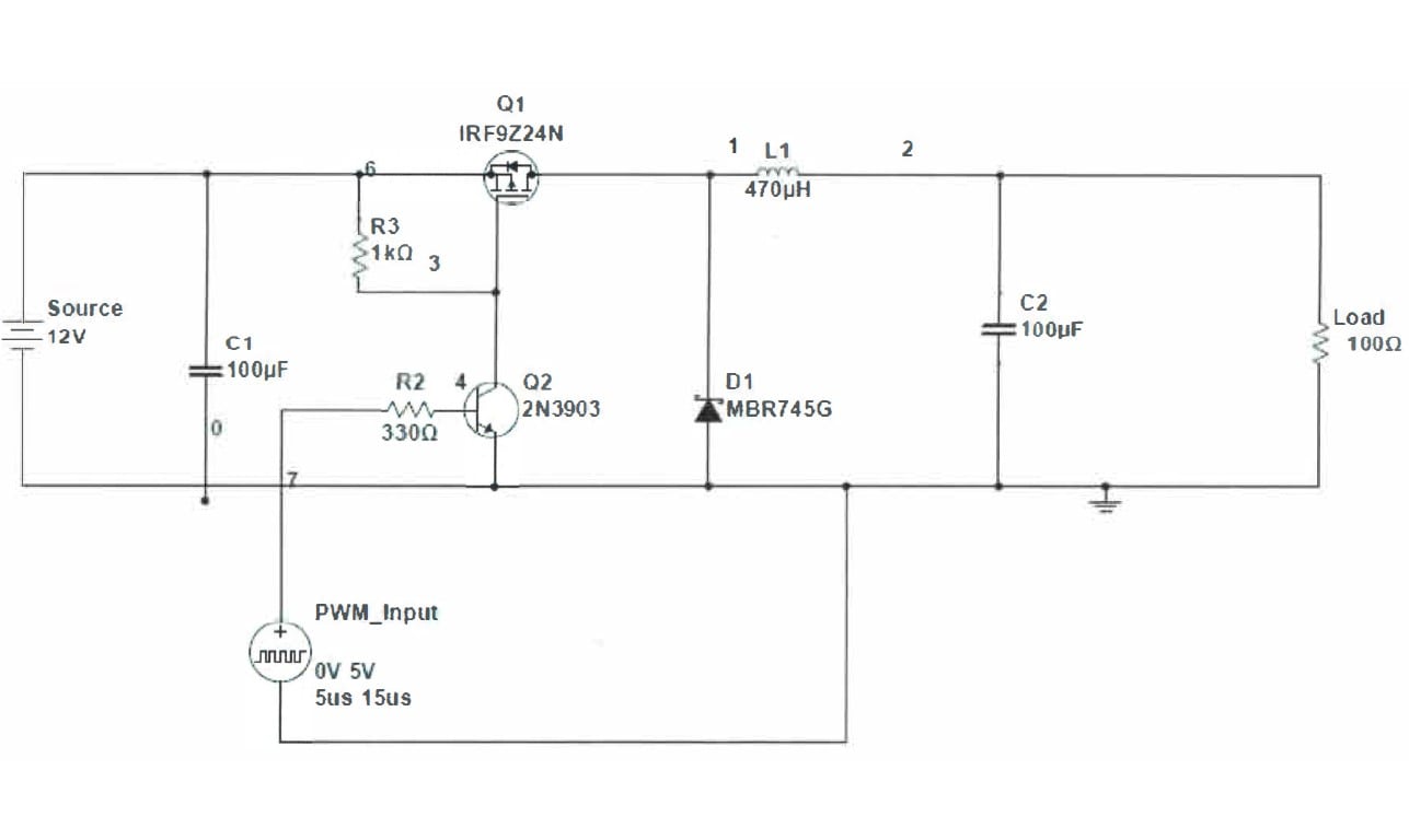
Circuit diagram of boost converter From Fig. 3, during the switch

Download scientific diagram | Circuit diagram of boost converter From Fig. 3, during the switch is closed [10]; Vs is constant supply voltage, Vs = VL= L × (di/dt) (5) During the switch S is open; VS = VL + VC (6) Then, L × (di /dt) = VS-VC; di/dt = (VS-VC) / L Current increment when switch closed for duty cycle D; Imax-Imin = (VS /L) × D×T (7) Current decrement when switch open, Imin-Imax = (VS-VC) / L × (1−D) ×T (8) from publication: Performance of closed loop SEPIC converter with DC-DC converter for solar energy system | The Non-Conventional sources such as solar energy has been replacement and best exploited electric source. The solar electric power required DC-DC converter for production, controllable and regulation of variable solar electric energy. The single ended boost converter has | DC-DC Converters, Solar Energy and Solar | ResearchGate, the professional network for scientists.

Understanding the Operation of a Boost Converter - Technical Articles
DC to DC Boost Converter Circuit (Part 5/9)
Understanding the Operation of a Boost Converter - Technical Articles
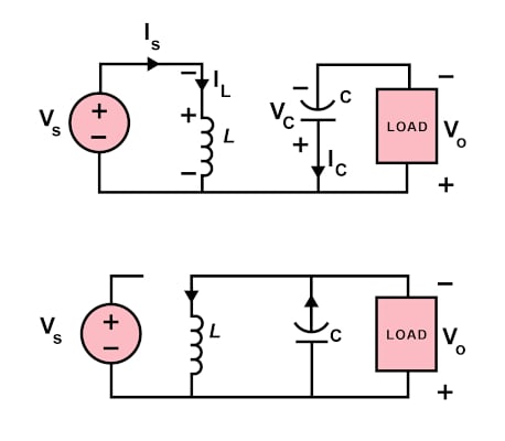
DC/DC Converters: Circuit Analysis–Intro to Predicting Circuit
High gain DC/DC converter with continuous input current for
USAFA - DC/DC Buck Converter Design Lab - Liquid Instruments
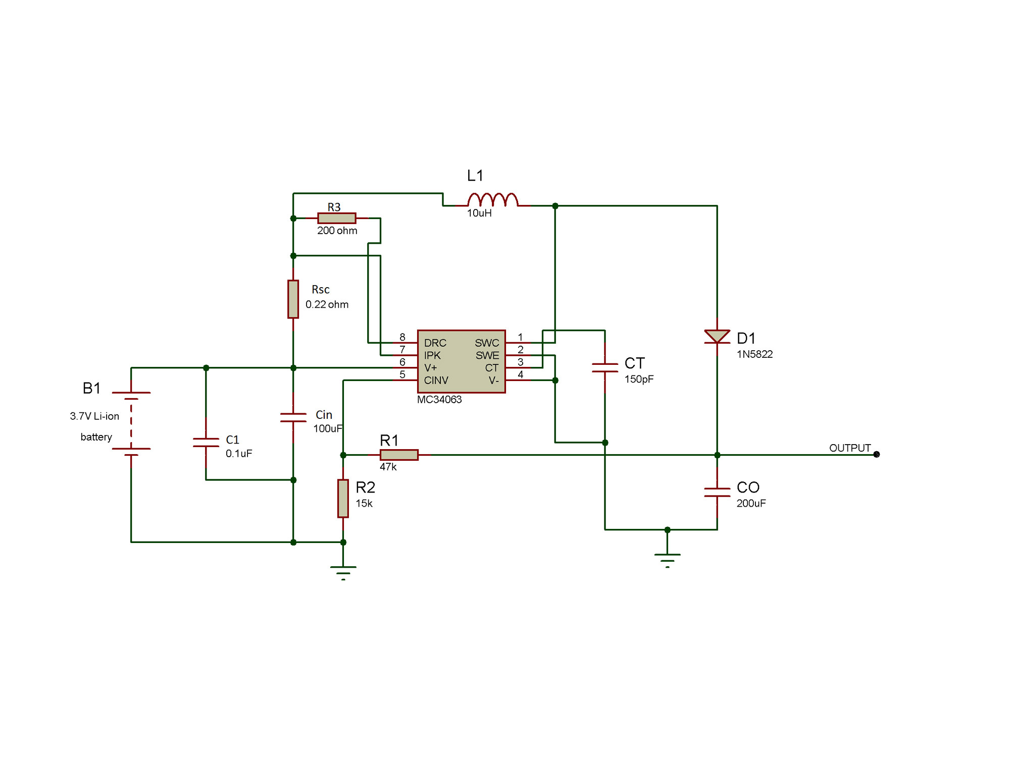
4 Easy Boost Converter Circuits Explained - Homemade Circuit Projects
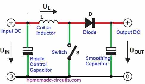
DC Voltage Converter Circuits
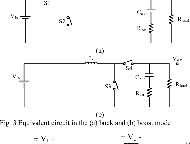
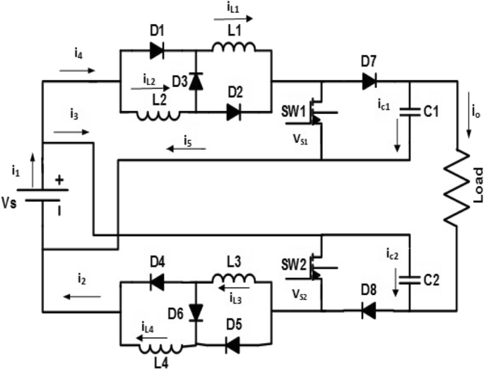
Figure 3 from Single-inductor four-switch non-inverting buck-boost
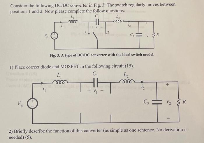
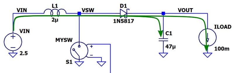
Solved Consider the following DC/DC converter in Fig. 3. The
A single-phase direct buck-boost AC–AC converter with minimum